Silicon Carbide Game-Changer: Aehr's Edge - SiC Pure Play $AEHR
By Dylan Patel — April 3, 2023
Source: https://semianalysis.com/2023/04/03/silicon-carbide-game-changer-aehrs/
Semiconductor manufacturing is the alchemical process of the modern era, a complex dance that requires the harmonious synchronization of thousands of companies and tens of thousands of process steps. Due to its complexity, yield is a more than $100 billion problem for the industry. As such, the fabrication process contains a constant stream of critical status checks to support the most complex thing humans have created.
A casual observer of the semiconductor industry will often over-focus on ASML and lithography, despite that only comprising ~22% of a semiconductor fab’s total equipment (in $ value). Metrology and inspection (checking) are ~13% of the tools (in $ value). Firms like KLA-Tencor KLAC -0.39%↓, Nova Measuring NVMI -1.12%↓, and Onto Innovation ONTO 0.66%↑ manufacture equipment that measures the wafer throughout the front-end.
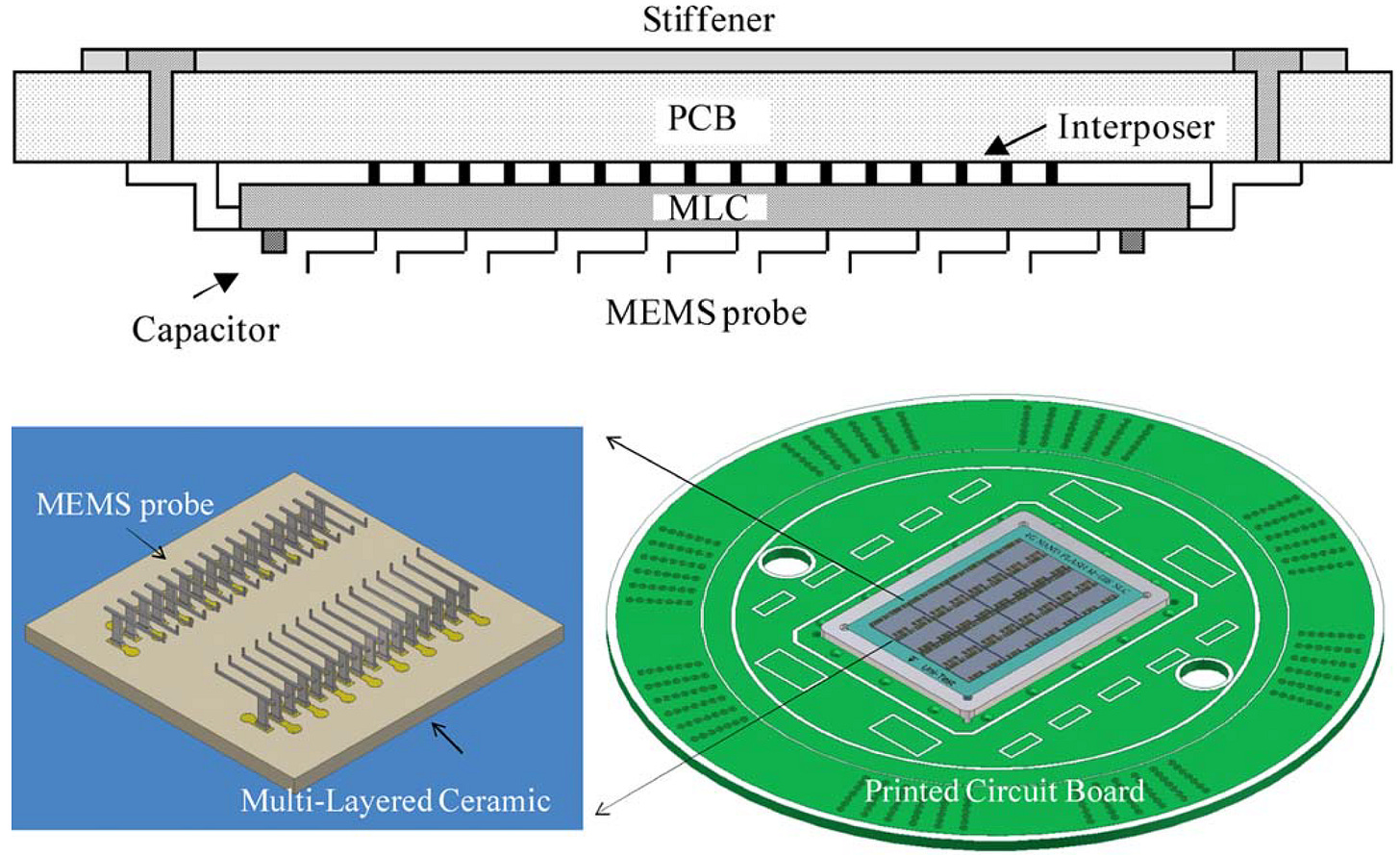
FormFactor FORM 1.02%↑, Micronics Japan 6871.JP, and Technoprobe TPRO.IT make probe cards that consist of a printed circuit board with an array of probes finer than a human hair. The arrangement of the probes is customized to every individual chip design. The probes themselves are so fine that they can only be manufactured on a MEMS wafer.
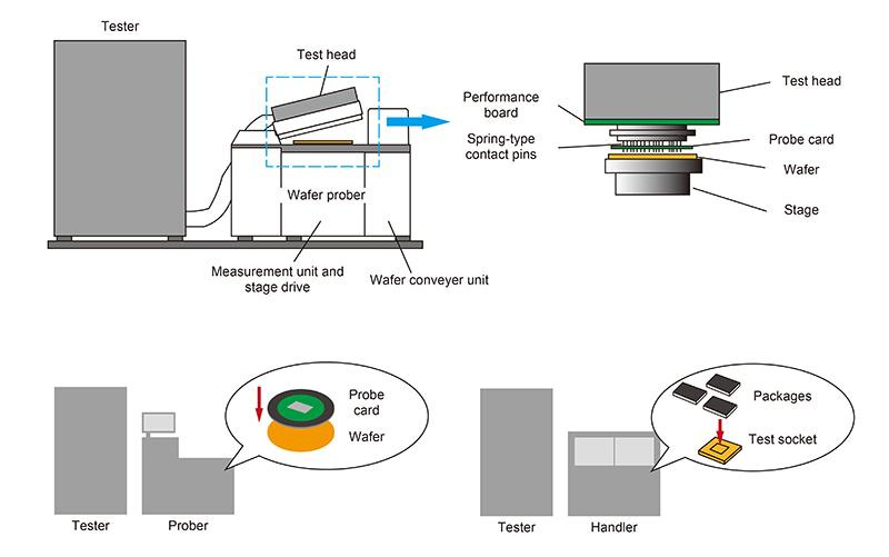
Advantest 6857.JP and Teradyne TER 0.57%↑ are most well-known for automated test equipment (ATE). Among many other things, ATE tools take the probe cards, line them up perfectly with the chips on the wafer, and make physical contact with the circuitry on the wafer. Then it sends precise electrical test signals to the circuits to characterize them.
That’s just a quick, incomplete summary of a few major firms, but there are many other firms in the “checking” industry. Today we want to discuss Aehr Test Solutions $AEHR, a small firm with a unique testing solution. It is used for Apple’s FaceID, Intel silicon photonics, and, most importantly, silicon carbide. We first published a report on the firm a couple of years calling out its early success in SiC. Since then, revenue and the stock price have soared due to the rapid adoption of their tools in silicon carbide. We have also participated in most earnings calls as analysts and visited their primary manufacturing facility.
Today’s report will dive into their unique test technology. We will explore the durability of Aehr’s competitive advantage versus multiple competitors and what those competitors are doing to reduce their technology gap with Aehr Test Systems. We will also include a model that considers EV requirements, tool throughput, consumables revenue ramp, test intensity, and more, indicating that Aehr’s opportunity is potentially more than $500 million annually. We will also discuss their potential for growth in GaN, silicon photonics, and memory devices. Lastly, we will discuss why Aehr is a better vehicle for long-term SiC and GaN growth versus Axcelis ACLS 0.82%↑ and Aixtron AIXA.

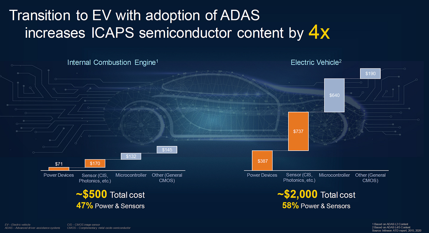
Due to its increased energy efficiency, Silicon carbide (SiC) is rapidly becoming the standard for high-power electronic devices. To support the explosion in electric vehicles, renewable energy, and energy storage, the industry is looking to increase wafer volume from a couple hundred thousand wafers a year to multiple million wafers a year by the decade’s end.
Failures in the electrification end markets are especially catastrophic because the automobiles and infrastructure are part of an installed base that should last decades. Furthermore, servicing and repair require taking apart a complex device in the field. These devices may function perfectly fine at normal temperatures when they are first fabricated, but failures and irregularities can become frequent over time when exposed to more extreme environments for an extended period.
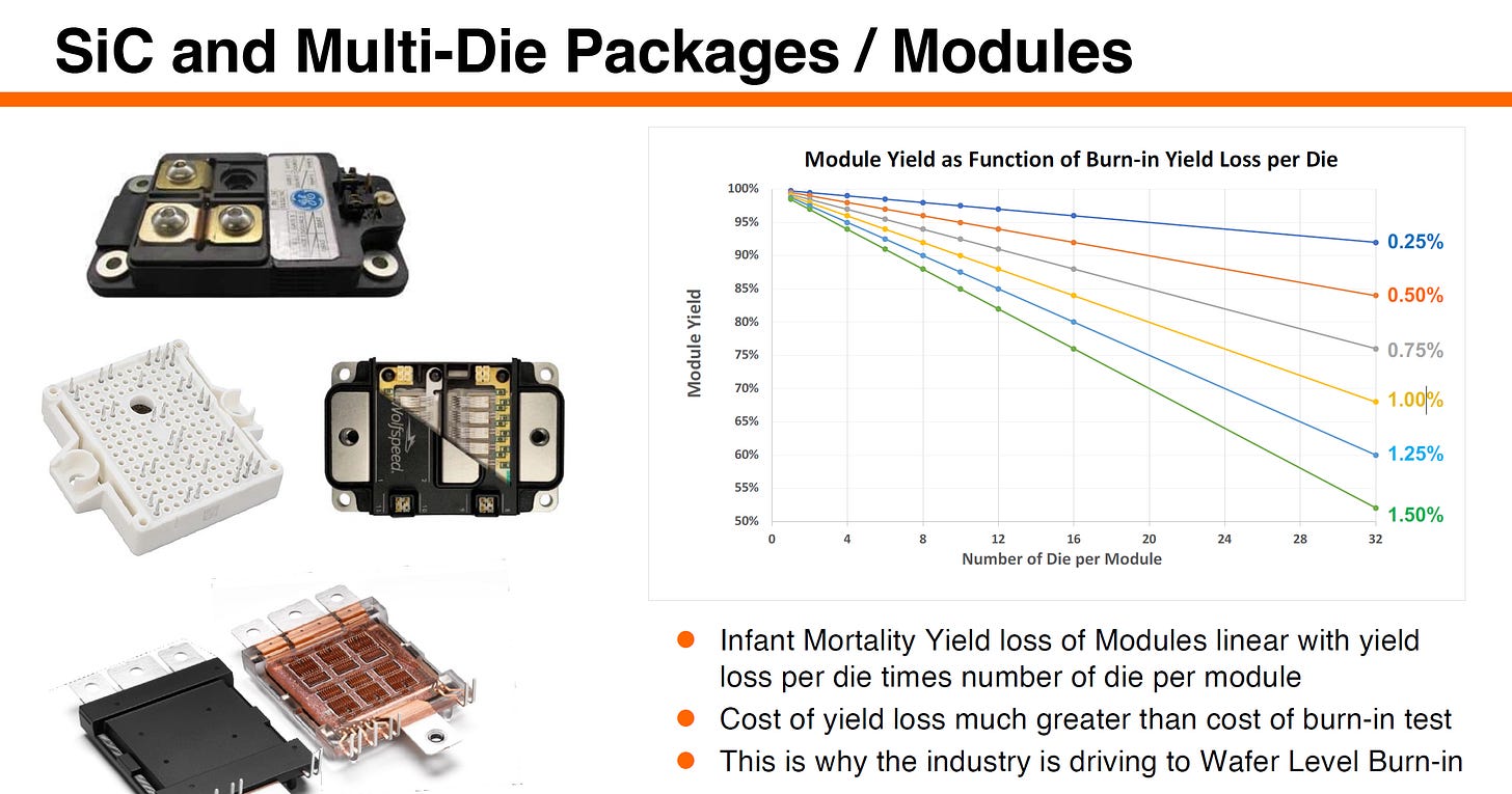
Automotive and industrial suppliers require intensive testing to become a qualified supplier, and even once qualified, there’s no skimping out on testing. SiC has many defects related to its fragile/brittle crystalline structure. Major sources include substrate, epi, or doping-related defects such as threading dislocations, ingrown stacking faults, and recombination-induced stacking faults (RISFs). Yield here is especially low relative to other semiconductors and contributes to about 30% of the final device cost. In-field defect rates take this figure much higher.

Testing in automotive can last two to four days per device, and the footprint required for testing thousands of devices is astronomical. Furthermore, most industry has moved from discrete power devices to multi-die modules. In these cases, even one bad die could cause many good dies to fail. With a decade-long failure rate of even 1%, the standard 12-die module will have a failure rate of ~15%!
The bathtub curve applies to semiconductors. Mortality rates are very high at the beginning of a device’s life cycle. This is called infant mortality. These high mortality rates exponentially decrease to a steady state. After a long period of low failure rates, failures eventually rise again due to wear-out failures. Infant mortality must be weeded out, but there are multiple ways to do so.

Most of the industry uses package or module burn-in to weed out infant mortality in high-value parts. Accelerated stress testing at elevated temp/voltages helps weed out rotting eggs by measuring any changes in the device’s performance during testing. These latent manufacturing defects can be pulled, minimizing the chances that a customer has a product die in the field. This is fine for the realm of IGBT and standard silicon-based devices because burn-in times are shorter, but with SiC, the costs begin to soar due to the length of burn-in time required. This is where Aehr Test System’s novel approach comes in. Instead of creating tools for testing on the module level, they make tools that test at the wafer-level.
The broader logic industry adopted an early version of these tools in the 90s, but then that transitioned away to more industry-standard testing. Aehr is still used for wafer-level burn-in for lasers, such as with Apple’s FaceID and Intel’s silicon photonics platform.

Due to poor yields with silicon carbide, a large portion of infant mortality can be weeded out. Allows fewer failed devices to be packaged and the full test cycle to be shortened. Cycle times are a major limiting factor in SiC device production, and Aehr's solution to decrease the cycle times is promising. On Semiconductor $ON is the first hallmark customer for Aehr in SiC. Aehr is also engaged with others such as Infineon, ST Microelectronics, Rohm, Wolfspeed, Mitsubishi, Rohm, Sanan IC, CR Micro, and more which we will discuss specific customer progress later.

The cost savings when moving to wafer-level burn-in are tremendous. If the automotive quality requirements hold, it is a no-brainer for every SiC device fabricator to move to wafer-level burn-in. As automakers become aware of it, some even require their vendors to implement very long burn-in of a dozen hours. As such, the only cost-effective way to do this is with Aehr.
Aehr has developed the FOX-XP tool for these wafer-level burn-in tests. Each wafer can contain as many as a thousand SiC devices. FOX-XP can test 9 to 18 wafers at a time. FOX-XP does this inside the chamber, which acts as a highly regulated extreme temperature environment. This can be considered an oven, except it, can dissipate over 18 kW too. The FOX-XP tools cost about $2.5M.
These tools must also be used with Aehr Test System’s WaferPak contactor. The WaferPak is similar to a probe card, but instead of only interfacing with the wafer, it also carries it. WaferPaks are considered a consumable as they are unique to each design and cost around $1.5M to fill out a FOX-XP. Designs typically change every few years. These design changes increase efficiency and reduce costs for end-market power devices.
![]()
Dylan Patel@dylan522p
Important to note on Tesla Silicon Carbide reduction, this is pretty much all tech advancement to new SiC from old. STMicroelectronics, their primary supplier, has considerably reduced area on their new architecture, from 2018 to 2022, a ~60% area reduction. Tesla timescale means… https://t.co/Mv3aCvDti6

9:08 PM · Mar 2, 2023
11 Reposts · 63 Likes
WaferPaks are a critical engine for future reoccurring revenue. Our model, which we will share later, indicates that WaferPaks will exceed FOX-XP revenue within a handful of years.
The WaferPak has 2048 I/O pins and DPS channels. Each channel has remote voltage and ground sense. Each channel can cycle between 1024 voltage levels up to 40V and as low as -30V. It can run as high as 2A. To be clear, WaferPaks aren’t capable of as fine-grained testing as a high-end probe card because they have significantly fewer probes. Furthermore, these probes have far finer control than high-end ATE equipment. The critical point is that it allows for high-voltage testing while operating at temperatures as high as 150 degrees Celsius.

The burn-in tools are capable of multiple types of tests. This includes bipolar voltage with negative high-temperature gate bias, which was requested and developed rapidly for one of the new customers.
The last piece is Aehr’s product line, the FOX-XP WaferPak Aligner, which vacuum suction loads and unloads wafers between FOUPs or wafer cassettes and the WaferPak Contactors. WaferPak Aligners generally cost less than $1M, but there are various offerings depending on the fab's automation requirements. Aligners can support multiple Fox-XP tools, but many fabs will want to completely automate Fox-XP, which requires pairing them 1 to 1 with fully automated aligners.
Next, we will discuss Aehr’s specific wins with Onsemi and the status of orders/sales with Infineon, ST Microelectronics, Rohm, Wolfspeed, Mitsubishi, Rohm, Sanan IC, and CR Micro. Furthermore, we will share our detailed model that shows industry-level demand for wafers with electrification and burn-in tool requirements. This model also separately models WaferPak and Aligner sales. Consumables are an essential part of Aehr’s story.
We will also discuss competition and their penetration into this space, including Pentamaster, EDA Industries, and Teradyne. We will also discuss their potential for growth in GaN, silicon photonics, and memory devices. Lastly, we will discuss why Aehr is a better vehicle for long-term SiC and GaN growth versus Axcelis $ACLS and Aixtron AIXA.
All of this is in the second half of the report below, for subscribers.
First off, customers. Onsemi is the first customer. We believe Infineon is their second customer and will come with significant orders over the next few quarters. Furthermore, we believe Mitsubishi Japan is another customer. Note that their large orders will come a good bit later because the full-scale manufacturing fab is still under construction. Samsung also has a sizable new SiC program and is interested in Aehr’s tools. They have also begun ordering smaller-scale systems from Aehr. Chinese firms, specifically CRCC Micro and Sanan, are potential giants in SiC if they can ramp up. The China question on SiC is a big one that could significantly reduce SiC device margins if they succeed. They have had multiple discussions with Aehr, but no orders yet. Rohm also has interest and has tested wafers with Aehr at their applications lab.
The most prominent missing firm is ST Microelectronics. They were the first to ramp up SiC with Tesla. ST Micro has been a big supporter of EDA Industries tools for SiC burn-in. They are a packaged part burn-in company that sells packaged part systems to ST. EDA took all of the electronics of their package part burn-in system, put them sideways, and bolted them on top of a Semics prober to build a costly system that tests one wafer at a time on a prober (configured as a five-prober cluster). This isn’t cost-effective and has no chance outside of ST Micro.
With that said, ST Micro has allegedly begun to move very quickly on Aehr. Aehr has sold systems to ST Micro for a very long time for the FaceID sensor, but they have been pretty against it for SiC. An automotive company has begun asking about wafer-level burn-in due to Onsemi using it as a selling point, and ST Micro is seriously considering this now. If automakers require multi-hour burn-in, an EDA Industries tool would never work and would not be cost-effective. Given that Onsemi and soon Infineon will be pushing this as a selling point for superior quality, it is a true potential for lock-in.
We believe Wolfspeed uses Pentamaster, a packaged part burn-in firm out of Malaysia. This is even less competitive than EDA Industries than wafer-level burn-in. They have also made a prober-based engineering tool that can do a single wafer burn-in up to 720 dies. The system has to be manually loaded by hand, and it tests only one wafer in the same footprint as AEHR (up to 18 wafers). It's not a system that is going to ramp into production. Their second-generation tool does two wafers and may ramp with Wolfspeed. We don’t know of any association with Wolfspeed, particularly for wafer-level tests, outside of Aehr and Pentamaster. Aehr seems to indicate that the holdout customers are moving quickly; if they don’t, there will be significant cost disadvantages for those firms.
The 800-pound gorilla is Teradyne. We believe they will not enter this market due to the lock-in and IP protection Aehr has. Aehr’s patent portfolio is quite strong in wafer-level burn-in, including the WaferPak temperature control, contacting, electrical components, current protection, and portability across wafer sizes. Furthermore, developing wafer-level burn-in involves a high degree of customer-supplier engagement and customization. Lastly, the TAM in terms of tools is relatively small for SiC at ~$100M or less for every year except 2027 in our model. Before and after 2027, the market size for Fox XP falls back below $100M again.
The more critical angle is the consumables side. Those consumables require an installed base, which will be hard for Teradyne to penetrate. Furthermore, the IP protection is much stronger on that side because while wafer-level burn-in is decades old, the methods of burn-in and types of tests for high-power electronics and photonics are much newer and protected with more recent patents.
The consumables also make Aehr a stronger player in the SiC investment space. More than 2/3 of their long-term income would come from WaferPaks in our model. Other SiC plays like Axcelis and Aixtron are heavily dependent on Capex, which will start to fall off rapidly after the middle part of the decade as more output per tool can be achieved and the EV adoption curve begins to level out.
Both Axcelis and Aixtron have more competition from the giants of Applied Materials and Tokyo Electron as well, which Aehr does not. Furthermore, in ion implant for SiC, Japanese firm Ulvac is also a strong competitor. Aehr is virtually unopposed by major firms, and it seems unlikely they will be. Lastly, as a percentage of Aehr’s revenue and growth, China is smaller than the other two firms, so further tool bans will not affect them nearly as much.
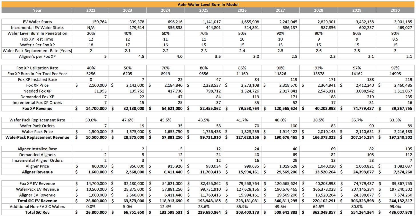
Next up is the model. There are many assumptions embedded here which we will explain first.
-
EV Wafer starts are specifically for silicon carbide demand from electric vehicles only. This figure includes assumptions around charging infrastructure and cars moving to SiC. This figure does not contain any assumptions or growth for non-EV SiC
-
Wafer-level burn-in penetration is for the customers who have adopted. Orders are placed for future production, not current demands. Furthermore, the current years do not align with Aehr’s actual business. Aehr did not have a 20% penetration in 2022, but they did take significant orders from Onsemi for equipment that will be utilized in future years. Furthermore, while the companies they have racked up as customers represent more than 40% of SiC in the future, they do not today, as ST Micro is the dominant player with nearly 50% share alone. They themselves have admitted their share will fall significantly over time.
-
Please note that we are not modeling Aehr’s current order book directly as timing will differ significantly, more so what the installed base would need to be from a bottoms-up perspective.
-
We project test time will fall somewhat as yields improve, but this will be buoyed somewhat by certain automakers requiring minimum burn-in time.
-
WaferPaks are replaced on regular cadence with new SiC designs. This will be much higher now, as the cadence of new designs is every two years. Over time this will increase to a three years cadence for new designs. The industrial market will mainly utilize designs that last much longer. In the 2030s, we expect designs to continue to lengthen and for most designs to stick around for much longer than even three years.
-
We assume utilization of Fox XP systems is relatively low currently due to excessive characterization and the somewhat more manual process with aligners. As time passes, utilization will increase meaningfully.
-
Aligners per Fox XP system are quite low, but as utilization rates increase and the ramp of fully automated tools are mated to individual Fox XP systems occurs, this will decrease over time, offering another avenue for revenue growth.
-
Non-EV SiC is significantly lower confidence from us. We have no ground-up modeling to support the non-EV renewable energy and energy storage markets. Obviously, they will also need higher efficiency SiC, but we are not sure about the amount. Give very little credence to this section.
![]()
Aehr Ground Up Model
24.4KB ∙ XLSX file
Download
Download
Here is the file for the model as well. Use it as a base for how ground-up works. Note that while revenue spikes to as high as $500M in 2027, that includes 50% nebulous non-EV SiC. The number of non-EV SiC wafers other analysts are projecting is even higher, but we can’t understand the math behind it, so we want to discount that. Even on an EV-only basis, if Aehr’s solution gets broad adoption, that is more than $200M of WaferPak consumables revenue annually with minimal non-EV SiC revenue.
We believe Aehr can support this business level without much Capex. Aehr is a very Capex-light business due to its use of CMs for sub-components and its existing large facility. They do a large amount of in-house manufacturing, so it’s not like the CMs can easily leak IP. Having seen their facility, they could easily ship many more systems than they currently do. We believe it could support ~50 Fox XP systems a year before needing an additional facility. That is by doing eight systems simultaneously with a manufacturing time of 2 months.
The angle we aren’t sure about is the capacity for supporting enough WaferPaks. Their floor space for WaferPak was relatively small. They have significant unused/storage space that could be converted for the WaferPak in the current facility.
Also, here is a bit of chicken scratch for other sectors.
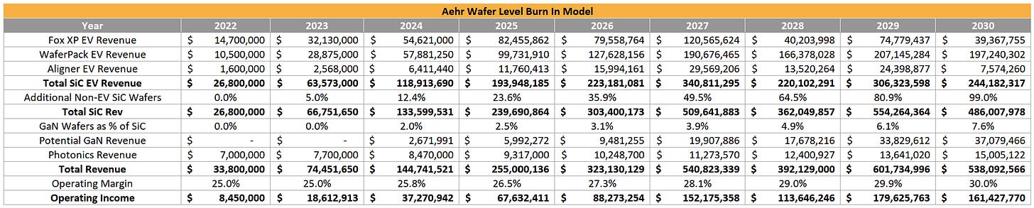
We do not hold much credence to Aehr’s argument that Photonics will be a significant growth driver, hence low revenue growth from us. The burn-in times are incredibly low, on the order of a few minutes per wafer. Even if hundreds of thousands of wafers have hybrid lasers for co-packaged optics, which is incredibly unlikely, the number of tools needed to support this is very low. The number of WaferPaks could be high though, if many desperate designs use hybrid lasers. Lidar and FaceID applications are not going to drive much business. Most likely, external lasers are used for SiPho or in standardized co-packaged optical tiles.
High-power GaN devices, especially in industrial segments, are a powerful angle for success. GaN is very early and could even upset SiC in certain areas. The bipolar voltage with negative high-temperature gate bias developed for/with Infineon will also be used for their industrial and EV GaN solutions.
It is improbable for consumer-grade GaN to adopt wafer-level burn-in as those are low enough power to be discrete devices, not packaged modules, and the testing intensity requirements are much lower. Only datacenter GaN or other high-power GaN applications are worth doing wafer-level burn-in. The few non-EV areas where they could see success may be a substitute for SiC. The critical growth area is enabling new use cases and eating IGBT share. Those new use cases include RF. SiC and GaN have some potential there, although it isn’t clear how that shakes out yet. We could easily imagine a world where every solar panel/wind installation or 6G RF requires this type of burn-in, but that is all imagination, not grounded in technical demonstrations.
Aehr has excellent operating margins for their scale, and as such, they will be near industry-leading as they keep scaling. The earnings power of Aehr is powerful, and they deserve a valuation with a $1 billion handle long term.

Book a meeting with SemiAnalysis
Schedule a meeting
Book meeting